
Hi Jean-Samuel, Harald, Holger,
I've been quite for a while, so I want to make an update about the state of our hardware.
On the FPGA development side we've been stuck for ~3 weeks, because somethings happened with the power controller on our Xilinx SP-605 board and we've been waiting for TI's USB-TO-GPIO to flash this controller. And now we're still dealing with this problem.
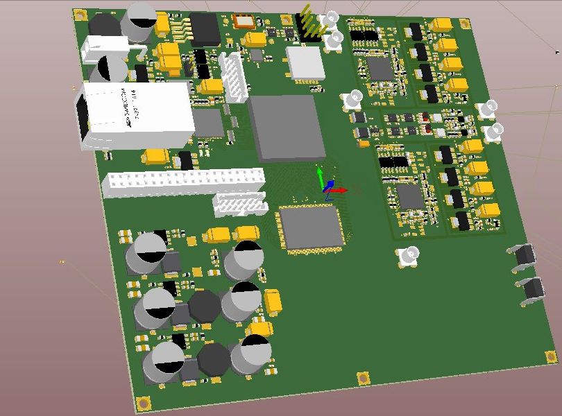
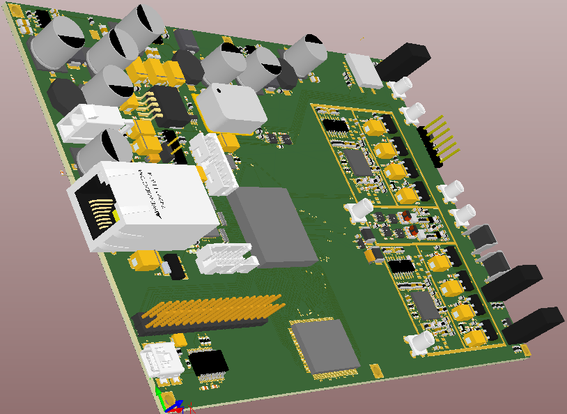
On the hardware side things are much better. We have "Release Candidate" of schematics and working on PCB layout. We estimate that layout will be finished in a week if we don't decide to change something too much. In attachment you could find the latest versions of schematics in PDF and Altium Designer formats, 3D view (pre-alpha version), list of FPGA I/O and BOM. I would very much appreciate any comments, questions, concerns and ideas about schematics, controls placement, debug facilities, etc. It's much, much better to find bugs and satisfy all requests now, then when we get PCBs printed.
Following the idea of Jean-Samuel we're trying to fit the PCB into 5.25" form-factor to be able to use various standard enclosures and even mount the board into a standard PC cases instead of a CD-ROM drive :) Right now estimated board size is 135х170mm, which perfectly fits into 5.25" case.
Meantime I've created Google Code project to host our development: http://code.google.com/p/umtrx/ It's empty yet, I plan to gradually fill it with information. I'm happy to grant member rights for the project to any of you who is willing to contribute to descriptions, code (not there yet), etc. Just drop me an e-mail when you feel you need those rights.
Hi all,
Attached is a new version of our schematics and PCB layout (note, they may differ a bit with schematics being more recent).
Btw, I found diffpdf tool very useful for schematics comparison: http://www.qtrac.eu/diffpdf.html It nicely highlights changes, so you don't miss something.
Our current plan for hardware prototyping is like this:
1. Most important parts of PCB layout should be done by the end of this week 2. Then we have 1 week (maximum!) to do any small changes to layout we may want and fix bugs we (hopefully) find. 3. Then 1 week for the final layout polishing, adding labels, etc. 4. Final ACK for the layout and we push it to the fab for printing. Manufacturing and delivery to Moscow will take 2-3 weeks. 5. 1 week for assembly
This is about 5-7 weeks and then we will have a lot of fun with hardware and software debug.
Robin, do you want to get an assembled board to participate in the hardware debug session? :) Btw, could you get a quote for the FPGA from Xilinx for 100pcs?

Hi Alexander. Yes, I'd definitely be interested in participating in a hardware debug session. I have a long-term FPGA consulting gig for Analog Devices and may be able to get permission to use some of their high-end test Agilent equipment in the lab on evenings and weekends if I ask nicely.
I just e-mailed my outside sales guy at Avnet and requested a quote for the XC6SLX75-2FGG484Chttp://avnetexpress.avnet.com/store/em/EMController/FPGA/Xilinx/XC6SLX75-2FGG484C/_/R-9951687/A-9951687/An-0?action=part&catalogId=500201&langId=-1&storeId=500201&listIndex=-1 qty. 100 and 1000. (I'll also get a quote from Arrow for a comparable Altera part, which will be useful in negotiating a better price than the one they will initially offer.)
In my spare time over the next couple of months, I'm going to attempt to add support for a 10/100 Ethernet MAC in the USRP N210 FPGA image.
-Robin
On Tue, Oct 4, 2011 at 5:45 PM, Alexander Chemeris < alexander.chemeris@gmail.com> wrote:
Hi all,
Attached is a new version of our schematics and PCB layout (note, they may differ a bit with schematics being more recent).
Btw, I found diffpdf tool very useful for schematics comparison: http://www.qtrac.eu/diffpdf.html It nicely highlights changes, so you don't miss something.
Our current plan for hardware prototyping is like this:
- Most important parts of PCB layout should be done by the end of this
week 2. Then we have 1 week (maximum!) to do any small changes to layout we may want and fix bugs we (hopefully) find. 3. Then 1 week for the final layout polishing, adding labels, etc. 4. Final ACK for the layout and we push it to the fab for printing. Manufacturing and delivery to Moscow will take 2-3 weeks. 5. 1 week for assembly
This is about 5-7 weeks and then we will have a lot of fun with hardware and software debug.
Robin, do you want to get an assembled board to participate in the hardware debug session? :) Btw, could you get a quote for the FPGA from Xilinx for 100pcs?
-- Regards, Alexander Chemeris.
Robin,
On Wed, Oct 5, 2011 at 05:33, Robin Coxe coxe@close-haul.com wrote:
Hi Alexander. Yes, I'd definitely be interested in participating in a hardware debug session. I have a long-term FPGA consulting gig for Analog Devices and may be able to get permission to use some of their high-end test Agilent equipment in the lab on evenings and weekends if I ask nicely.
Thank you! This may be very helpful.
I just e-mailed my outside sales guy at Avnet and requested a quote for the XC6SLX75-2FGG484C qty. 100 and 1000. (I'll also get a quote from Arrow for a comparable Altera part, which will be useful in negotiating a better price than the one they will initially offer.)
Thanks! Looking forward to see their quotes.
In my spare time over the next couple of months, I'm going to attempt to add support for a 10/100 Ethernet MAC in the USRP N210 FPGA image.
That would be truly great. Keep us updated.
Hi Alexander. I took a look at the schematic last night. Protel is hard for me to read, probably because I'm not used to it. Overall, the board looks very nice. I have a couple of questions/comments:
1) Is there a particular reason why there's an external SRAM on the board? I notice that there is one on the Ettus N210 board as well, but do guys have a particular purpose in mind for it? The Spartan-6 FPGA has ample on-board Block RAM resources. If it's not strictly necessary, it would remove an ~$10 part from the BOM.
2) Maybe it was just because it was really late, but I couldn't figure out what was happening to the 1 PPS GPS timing pulse. How are you planning to use GPS information to discipline the 26 MHz oscillator?
3) One general recommendation: add lots of test points, particularly around the DC power sources, clock signals, and digital signals of interest going to and from the FPGA. Probing BGAs is a pain without them. Also, strategically placed ground test posts that you can use to clip on a scope probe ground connection will make debugging much easier.
4) 6.5 V is kind of a weird voltage. I'd be inclined to go with a 12V connection to an external power source, which would enable the system to be powered off a car battery, but this point is a matter of opinion more than anything else.
-Robin
On Tue, Oct 4, 2011 at 5:45 PM, Alexander Chemeris < alexander.chemeris@gmail.com> wrote:
Hi all,
Attached is a new version of our schematics and PCB layout (note, they may differ a bit with schematics being more recent). Btw, I found diffpdf tool very useful for schematics comparison: http://www.qtrac.eu/diffpdf.html It nicely highlights changes, so you don't miss something.
Our current plan for hardware prototyping is like this:
- Most important parts of PCB layout should be done by the end of this
week 2. Then we have 1 week (maximum!) to do any small changes to layout we may want and fix bugs we (hopefully) find. 3. Then 1 week for the final layout polishing, adding labels, etc. 4. Final ACK for the layout and we push it to the fab for printing. Manufacturing and delivery to Moscow will take 2-3 weeks. 5. 1 week for assembly
This is about 5-7 weeks and then we will have a lot of fun with hardware and software debug.
Robin, do you want to get an assembled board to participate in the hardware debug session? :) Btw, could you get a quote for the FPGA from Xilinx for 100pcs?
-- Regards, Alexander Chemeris.
On Wed, Oct 5, 2011 at 17:50, Robin Coxe coxe@close-haul.com wrote:
Hi Alexander. I took a look at the schematic last night. Protel is hard for me to read, probably because I'm not used to it. Overall, the board looks very nice. I have a couple of questions/comments:
- Is there a particular reason why there's an external SRAM on the board?
I notice that there is one on the Ettus N210 board as well, but do guys have a particular purpose in mind for it? The Spartan-6 FPGA has ample on-board Block RAM resources. If it's not strictly necessary, it would remove an ~$10 part from the BOM.
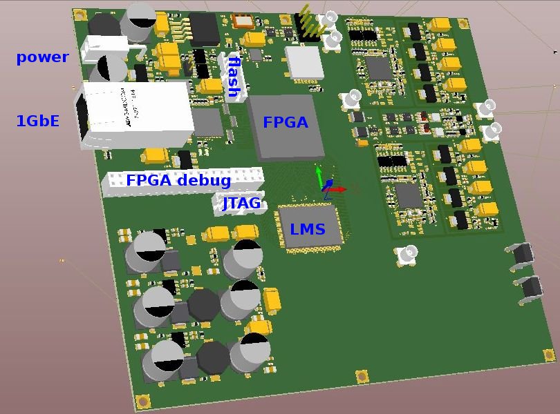
It's used as a FIFO for TX packets with timestamps. I.e. if your packet has timestamp in future it will be stored in this RAM for a while. It's 9MBit RAM, so Block RAM can't compete with it here. Whether this is strictly needed or is still open - we didn't do deep investigation. We may remove it later or just not populate if decide it's not needed.
- Maybe it was just because it was really late, but I couldn't figure out
what was happening to the 1 PPS GPS timing pulse. How are you planning to use GPS information to discipline the 26 MHz oscillator?
It goes to FPGA and then we have to implement PID controller there which will pull TCXO by adjusting DAC output (DAC121S101CIMK). We haven't done any work on this yet, because PID regulator coefficients must be tuned to specific DAC/TCXO and for testing purposes we can tune manually. I saw PID regulator at OpenCores, so I don't think its implementation is a big deal - tuning will take time OTOH.
- One general recommendation: add lots of test points, particularly around
the DC power sources, clock signals, and digital signals of interest going to and from the FPGA. Probing BGAs is a pain without them. Also, strategically placed ground test posts that you can use to clip on a scope probe ground connection will make debugging much easier.
Yeah, I'm going to talk with Andrey about debugability tomorrow.
- 6.5 V is kind of a weird voltage. I'd be inclined to go with a 12V
connection to an external power source, which would enable the system to be powered off a car battery, but this point is a matter of opinion more than anything else.
This is a good question. I think we decided that it doesn't matter much will the power dissipate at our board or at external converter when converting 12V to 6V. But we're open to discussion about this, as I believe it's an important point.
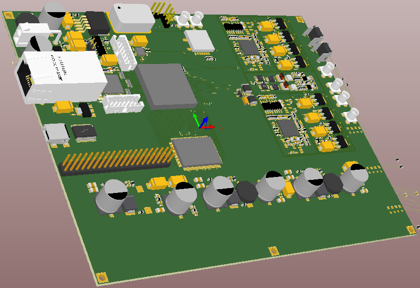
The latest version is attached. Looking forward to your comments.
Andrey will try to add one more converter to support 10-14V to be able power it from batteries in the next revision.
Regarding test-points - we'll add more test points for LMS. Robin, if you could recommend any specific points to check, we'll try to add them.
Hi all,
We're going to start the last iteration of PCB layout today and thus if you have any comments, it's better to write them right now. Otherwise it will be harder to incorporate them.
On Fri, Oct 7, 2011 at 02:28, Alexander Chemeris alexander.chemeris@gmail.com wrote:
The latest version is attached. Looking forward to your comments.
Andrey will try to add one more converter to support 10-14V to be able power it from batteries in the next revision.
Regarding test-points - we'll add more test points for LMS. Robin, if you could recommend any specific points to check, we'll try to add them.
-- Regards, Alexander Chemeris.

Hi Alexander,
I looked at the schematics and PCB. I did not notice anything bad. However, I am not really able to check everything.
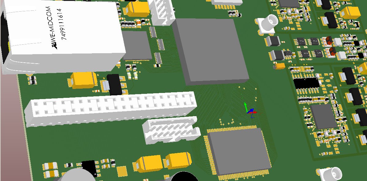
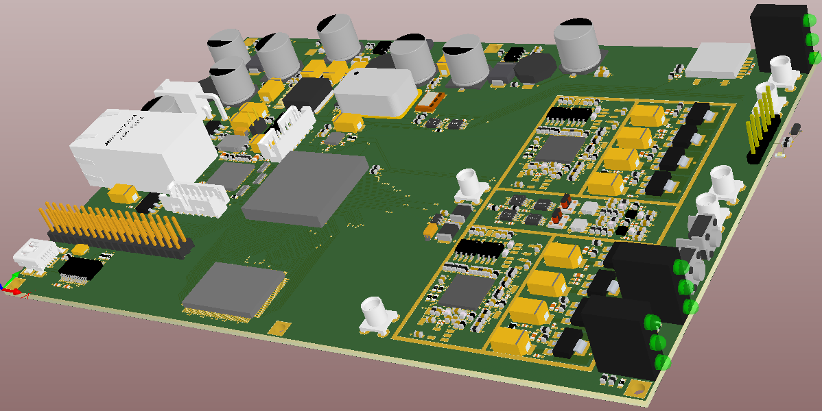
Anyway, I just have two questions. 1/ There is a CLKIO connector. As I can see on the schematics. We can set this as a clock output (master) or input (slave). This looks perfect if we want to synchronize 2 boards together (1 master output connected to 1 slave input). If we need to synchronize 3 boards together (trisector configuration), how could we connect them together ? Can we split the clock output signal to connect it to the 2 slave inputs ? If yes, everything is fine. If not, we might need 1 ouput and 1 input on the board (instead of 1 output or 1 input) to allow us to daisy chain the boards. What do you think ? 2/ On Image2, I can see 3 components outside the board near the 6 pin connector. Is this normal ?
Please let me know about these two points.
Best regards.
Jean-Samuel. :-)
On Tue, Oct 11, 2011 at 4:41 AM, Alexander Chemeris < alexander.chemeris@gmail.com> wrote:
Hi all,
We're going to start the last iteration of PCB layout today and thus if you have any comments, it's better to write them right now. Otherwise it will be harder to incorporate them.
On Fri, Oct 7, 2011 at 02:28, Alexander Chemeris alexander.chemeris@gmail.com wrote:
The latest version is attached. Looking forward to your comments.
Andrey will try to add one more converter to support 10-14V to be able power it from batteries in the next revision.
Regarding test-points - we'll add more test points for LMS. Robin, if you could recommend any specific points to check, we'll try to add them.
-- Regards, Alexander Chemeris.
-- Regards, Alexander Chemeris.
Hi Jean-Samuel,
On Tue, Oct 11, 2011 at 17:11, Jean-Samuel Najnudel - BJT PARTNERS SARL jsn@bjtpartners.com wrote:
Hi Alexander,
I looked at the schematics and PCB. I did not notice anything bad. However, I am not really able to check everything.
Anyway, I just have two questions. 1/ There is a CLKIO connector. As I can see on the schematics. We can set this as a clock output (master) or input (slave). This looks perfect if we want to synchronize 2 boards together (1 master output connected to 1 slave input). If we need to synchronize 3 boards together (trisector configuration), how could we connect them together ? Can we split the clock output signal to connect it to the 2 slave inputs ? If yes, everything is fine. If not, we might need 1 ouput and 1 input on the board (instead of 1 output or 1 input) to allow us to daisy chain the boards. What do you think?
Andrey says we can connect 3 to 5 units to a single output easily. We just need to make a "splitter-cable".
2/ On Image2, I can see 3 components outside the board near the 6 pin connector. Is this normal ?
Yes this is normal, as layout is not 100% finished yet. If there is no serious objections or additions, we're going to start final layout iteration immediately. It will take about a week more to polish everything.
Hi Alexander,
Thank you very much for your reply. In this case, it looks good.
Best regards.
Jean-Samuel. :-)
On Tue, Oct 11, 2011 at 3:16 PM, Alexander Chemeris < alexander.chemeris@gmail.com> wrote:
Hi Jean-Samuel,
On Tue, Oct 11, 2011 at 17:11, Jean-Samuel Najnudel - BJT PARTNERS SARL jsn@bjtpartners.com wrote:
Hi Alexander,
I looked at the schematics and PCB. I did not notice anything bad.
However,
I am not really able to check everything.
Anyway, I just have two questions. 1/ There is a CLKIO connector. As I can see on the schematics. We can set this as a clock output (master) or input (slave). This looks perfect if
we
want to synchronize 2 boards together (1 master output connected to 1
slave
input). If we need to synchronize 3 boards together (trisector configuration), how could we connect them together ? Can we split the
clock
output signal to connect it to the 2 slave inputs ? If yes, everything is fine. If not, we might need 1 ouput and 1 input on the board (instead of
1
output or 1 input) to allow us to daisy chain the boards. What do you
think?
Andrey says we can connect 3 to 5 units to a single output easily. We just need to make a "splitter-cable".
2/ On Image2, I can see 3 components outside the board near the 6 pin connector. Is this normal ?
Yes this is normal, as layout is not 100% finished yet. If there is no serious objections or additions, we're going to start final layout iteration immediately. It will take about a week more to polish everything.
-- Regards, Alexander Chemeris.
-
 Alexander Chemeris
 -
 Jean-Samuel Najnudel - BJT PARTNERS SARL
 -
 Robin Coxe