
I just recently made some changes to my 1.4 firmware to support Man-in-the-Middle modification of ATR because some device apparently changes the Vcc to 1.8v after reading the ATR that indicates the card supports Class C. I don't have access to the device that exhibit this behavior so I was using a USB Smartcard reader to test it, and my Oscilloscope capture shows that the PC was using 5v vddio mode. The SIMtrace 1 are 5v tolerant, and the last time I looked at Cstartup.asm I believe we set the internal pull-ups to disabled, which is "safe" according to the Atmel part documentation. So long as 5v IO levels are not "on"/"fed" into the PIO lines while the device is in reset, this is probably not an issue for SIMtrace 1 boards.
From: Mychaela Falconia mychaela.falconia@gmail.com To: simtrace@lists.osmocom.org Cc: Bcc: Date: Tue, 25 Oct 2022 20:03:23 -0800 Subject: My progress with 5V SIM investigation Hello SIMtrace community,
I mentioned earlier on this list, and also in last week's OsmoDevCall, that I play with some old phones that *may* be putting out 5V toward the SIM, which SIMtrace2 hw does not tolerate - 5V exceeds the absolute maximum rating spec of SAM3S chip.
As the first step in the investigation, I cobbled together a simple PCB design for a purely passive adapter that connects a SIM socket to FPC cables from current Sysmocom SIMtrace kits, plus 2.54 mm headers on both sides of the SIM socket providing convenient probing access to all signals. This trivial design can be found in my fc-small-hw Hg repository:
https://www.freecalypso.org/hg/fc-small-hw/
Look in the sim-fpc-pasv directory inside the Hg repo. I haven't sent this little PCB out to fab yet, but I plan on doing so when my budget allows it, hopefully no later than a week from now. When I get this adapter board fabbed and assembled, I will test it with my current collection of old phones (Ericsson I888, Nokia 5190 and 6190) and see if any of these phones put out 5V toward the SIM.
Nokia 5190 and 6190 are powered by 3-cell NiMH batteries, but they still might put out 5V toward the SIM if they include a charge pump or some other boost converter. At least in TI chipset history, prior to our well-known Calypso+Iota chipset, their previous ABB chip Nausica (used in the legendary TSM30, apparently) could put out either 3V or 5V toward the SIM, selection under fw control, while powered by a 3-cell NiMH or 1-cell Li-ion battery, doing some kind of boost conversion for 5V. (I never found a datasheet for that ancient ABB, so I don't know the full details.) It will be interesting to know what Nokia 5190 and 6190 do in this regard. It will also be interesting to see what Ericsson I888 puts out: it is an older, higher-voltage beast, powered by a 4-cell NiMH battery, and if the designers felt like operating the SIM in "5V" or Class A mode, they could have used raw battery voltage without conversion, as the spec is 4.5 V minimum IIRC.
During last week's OsmoDevCall Kevin said that he had some SIMtrace1 boards with ARM7S, which the datasheet says is 5V-tolerant, and I recall him saying that he could send me one. To Kevin: I greatly appreciate your offer, and I may indeed take you up on it in another few weeks - but let me build my sim-fpc-pasv adapter first, and see what voltages are actually put out by phones in my collection.
Now the really interesting phone would be Nokia 2190 - supposedly one of the very first PCS1900 band GSM phones sold in USA, from around 1995. That one is powered by a 5-cell NiMH battery and thus seems very likely to put out 5V toward the SIM, possibly always, without ever switching down to 3V. I don't have one to test, aside from a sealed box which I am reluctant to cut open (told it may be worth a fortune some day, the usual story), but another person on Reddit says that these phones are very finicky in terms of which SIMs they accept. I sent him a few of my FCSIM1 cards, equivalent to sysmoSIM-GR2, a pure GSM 11.11 SIM without any UICC at all, very old-fashioned, and my contact tells me that Nokia 2190 rejects these SIMs too! It was my desire to use SIMtrace to see what's happening with that finicky 2190 that prompted my investigation into 5V tolerance - and when I get my sim-fpc-pasv adapter built, I will get back in touch with my Nokia 2190 contact person from Reddit and see how he would like to proceed.
M~ _______________________________________________ simtrace mailing list -- simtrace@lists.osmocom.org To unsubscribe send an email to simtrace-leave@lists.osmocom.org

Min Xu min.xu@min-info.net wrote:
I just recently made some changes to my 1.4 firmware to support Man-in-the-Middle modification of ATR because some device apparently changes the Vcc to 1.8v after reading the ATR that indicates the card supports Class C.
The very fact that you had to do this MITM modification indicates a flaw in the design of SIMtrace. A *correct* SIMtrace hw design would allow the phone to put out any of the 3 voltage classes (5V, 3V or 1.8V) in any order of the phone's choosing, be it spec-correct or spec-violating, would pass *all* of them through to the SIM transparently, and would reliably sniff the communication between the phone and the SIM in all 3 classes, whichever ends up being chosen. My primary use case for SIMtrace is debugging and troubleshooting phone-to-SIM compatibility problems, i.e., answering questions like why does phone model ABC reject SIM model XYZ, and the last thing we need is Heisenbug behaviour where the addition of SIMtrace alters the environment in any way.
I have a desire to design and build a new SIMtrace board with the following architecture:
[ASCII art block diagram follows; email needs to be read in a fixed width font for it to appear correctly.]
+-------------+ +-------+ | dual supply | | | | xlat buffer +-------+ | +-------------+ | | | | | | +---------------+ | | | | OD driver for | | | | | SIM I/O line +--+ | | +---------------+ | MCU | | | | | +---------+ | | | | | local | | | | +--+ SIM I/F |========+ | | | | | driver | S2 | | | +-------+ +---------+ | | | | | | | Phone ==+==+================================================+== SIM socket S1
The double horizontal line (made of ASCII '=' characters) in this block diagram represents the SIM bus, made up of 5 wires: Vcc, CLK, RST, I/O and Vpp. Yes, I know full well that Vpp has no actual use, but the existing FPC cables do bring it from the phone to the board, and my no-Heisenbugs approach is to connect it electrically to the SIM socket when the 4 actually-used lines are connected through for trace mode, as detailed below.
S1 and S2 are meant to be 5-pole, single-throw switches, or even better, a single 5-pole, dual-throw switch combining S1 and S2. S1 and S2 must never be closed (conducting) at the same time, only one or the other, although having both S1 and S2 open is a legitimate setting for modes in which the SIM socket is unused. My ideal vision of the switch component for S1/S2 would be something that functions just like a relay; I figure that using an actual relay would probably be insane, but I really want it to function like a relay, thus finding a suitable electrical switch (less power-hungry than a relay) would require some investigation.
The component identified as "dual supply xlat buffer" is envisioned as Nexperia 74LVC4T3144, translating 3 signals unidirectionally from the any-voltage SIM interface to the fixed-voltage MCU; the 3 signals it will handle are CLK, RST and I/O. Notice that this path only allows the I/O line to be sniffed and not driven.
The component identified as "OD driver for SIM I/O line" is envisioned as Nexperia 74LVC1G07, or perhaps one half of a 74LVC2G07 if the other half will be used as part of the "local SIM I/F driver" block.
The "local SIM I/F driver" block will consist of a local 3.0 V supply to be fed to the SIM, a local LVC buffer for driving CLK and RST (inputs from MCU, proper 3.0V outputs to the SIM), a pull-up resistor to the local 3.0V supply on the I/O line, and the other half of 74LVC2G07 for driving this line in the proper OD manner. This local I/O line will also be connected directly to an MCU input.
I envision this device as being able to operate in 4 possible modes:
Trace mode: S1 closed, S2 open. The local SIM I/F driver block is electrically disconnected, the SIM is electrically connected to the phone, transparent to all 3 voltage classes, and the firmware must commit to NOT driving the OD buffer on the left side of the block diagram. In this mode the presence of SIMtrace should be invisible (no Heisenbug effect), and the firmware simply sniffs the output from 74LVC4T3144 translating buffer. The tracer will reliably sniff phone to SIM communication with proper Vih and Vil thresholds no matter which of the 3 classes is in use, and if we also connect phone VCC to an ADC input, the trace log can capture the sequence of which voltages the phone tried in which order.
Card emulation mode: both S1 and S2 open, on-board SIM socket unused. The MCU will receive CLK, RST and I/O from the phone through the 74LVC4T3144 and talk back to the phone on the I/O line through the OD buffer. This mode will once again work correctly no matter which voltage class is chosen by the phone.
Card reader mode: S1 open, S2 closed. In this mode the SIM will always be operated in class B, never A or C - but because it is now a private interface between our MCU and the SIM, not involving the phone, I find this B-only restriction perfectly acceptable. With S1 open, the phone is disconnected and out of the picture.
MITM mode: S1 open, S2 closed, and the board functions electrically just like in the card reader mode. But it is really the card reader mode and the card emulation mode combined, operating simultaneously: one USART will talk to the phone, the other will talk to the SIM. The phone can once again apply any of the 3 voltage classes, SIMtrace will receive from the phone and talk back to the phone through the same path as in the card emulation mode above, and at the same time the other USART will talk to the SIM. The physical SIM will operate in class B no matter which voltage class is used on the phone to MITM interface.
Now for the big gotcha: although I got the idea outlined above, I don't know when I will get around to turning it into reality as in finding specific parts, capturing schematics and spinning out a PCB. The reason is prioritization: I only got one of me, and right now my desire to build FC Venus board is a higher priority than this improved SIMtrace idea. Therefore, if anyone would like to beat me to it, please go ahead! I have spelled out my idea in some detail above so people can know what I have in mind, and if someone else feels like taking my block diagram design and turning it into reality, go for it!
M~

Dear Min,
On Mon, Nov 14, 2022 at 12:04:03PM -1000, Min Xu wrote:
I just recently made some changes to my 1.4 firmware to support Man-in-the-Middle modification of ATR because some device apparently changes the Vcc to 1.8v after reading the ATR that indicates the card supports Class C.
Can you please share/publish the related modifications to modify the ATR on-the-fly?
Thanks in advance!
Hi Harald
Thank you for the appreciation. The diff files are extracted from our vendor svn repository against original 0.5 git release
Diff1 contains all of the changes that I have previously made against 0.5 and I believe a majority has been merged. But since I wasn't sure of the state on the full repository I am including them again.
Diff2 contains a change to wdt.c to reboot the board on WatchDog timeout, and also added brownout interrupt handle to also reboot. They maybe set to reboot in original firmware, but my repository prior to this change had them indicating the Watchdog timeout by rapidly blinking the LEDs. Both modes will reboot with different blinking pattern (possibly hard to tell)
Diff3 is the majority of Man-in-the-Middle changes. As I mentioned long ago, there is a difference between the original 1.3/1.4 board vs our board in that the power relay for vcc-phone into vcc-sim is enabled by setting a '1' for the 'nPWRFWD' instead of clearing to 0. I left the pin-name as is so I can vaguely remember this fact. To actually work, Diff5 is needed.
Diff4 is just my compulsiveness to clean up the newline format used throughout. Because a log saved by putty looked like random newlines are added
Diff5 fixes the TCK byte in ATR if present and TA3 was modified.
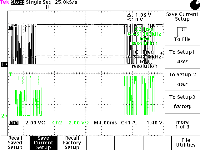
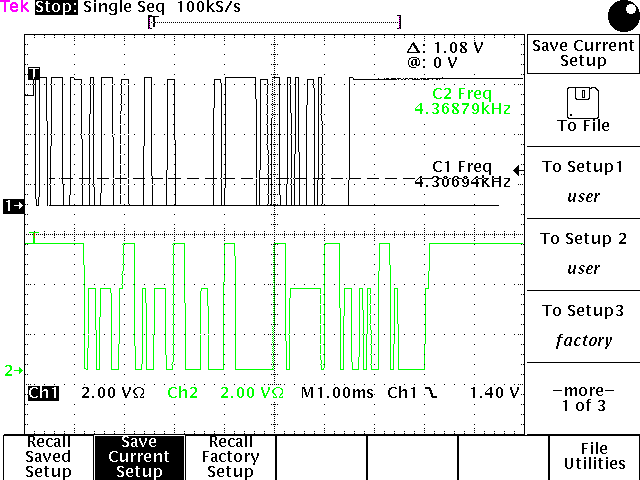
The two BMPs are part of Diff5 as a documentation of the Man-in-the-Middle result
Best Regards
On Thu, Nov 17, 2022 at 5:00 AM Harald Welte laforge@osmocom.org wrote:
Dear Min,
On Mon, Nov 14, 2022 at 12:04:03PM -1000, Min Xu wrote:
I just recently made some changes to my 1.4 firmware to support Man-in-the-Middle modification of ATR because some device apparently changes the Vcc to 1.8v after reading the ATR that indicates the card supports Class C.
Can you please share/publish the related modifications to modify the ATR on-the-fly?
Thanks in advance!
- Harald Welte laforge@osmocom.org http://laforge.gnumonks.org/
============================================================================ "Privacy in residential applications is a desirable marketing option." (ETSI EN 300 175-7 Ch. A6)
Oh in Diff3 there was also a bug fix for DI=8 and DI=9 handling in PPS process based on observed "unsupported baud rate" message, as well as handling the case where first PPS byte appears to be 00 similar to how ATR ignores initial 00 byte. As part of debugging PPS, printing the PPS REQ/RSP is added.
Min
On Thu, Nov 17, 2022 at 9:59 PM Min Xu min.xu@min-info.net wrote:
Hi Harald
Thank you for the appreciation. The diff files are extracted from our vendor svn repository against original 0.5 git release
Diff1 contains all of the changes that I have previously made against 0.5 and I believe a majority has been merged. But since I wasn't sure of the state on the full repository I am including them again.
Diff2 contains a change to wdt.c to reboot the board on WatchDog timeout, and also added brownout interrupt handle to also reboot. They maybe set to reboot in original firmware, but my repository prior to this change had them indicating the Watchdog timeout by rapidly blinking the LEDs. Both modes will reboot with different blinking pattern (possibly hard to tell)
Diff3 is the majority of Man-in-the-Middle changes. As I mentioned long ago, there is a difference between the original 1.3/1.4 board vs our board in that the power relay for vcc-phone into vcc-sim is enabled by setting a '1' for the 'nPWRFWD' instead of clearing to 0. I left the pin-name as is so I can vaguely remember this fact. To actually work, Diff5 is needed.
Diff4 is just my compulsiveness to clean up the newline format used throughout. Because a log saved by putty looked like random newlines are added
Diff5 fixes the TCK byte in ATR if present and TA3 was modified.
The two BMPs are part of Diff5 as a documentation of the Man-in-the-Middle result
Best Regards
On Thu, Nov 17, 2022 at 5:00 AM Harald Welte laforge@osmocom.org wrote:
Dear Min,
On Mon, Nov 14, 2022 at 12:04:03PM -1000, Min Xu wrote:
I just recently made some changes to my 1.4 firmware to support Man-in-the-Middle modification of ATR because some device apparently changes the Vcc to 1.8v after reading the ATR that indicates the card supports Class C.
Can you please share/publish the related modifications to modify the ATR on-the-fly?
Thanks in advance!
- Harald Welte laforge@osmocom.org http://laforge.gnumonks.org/
============================================================================ "Privacy in residential applications is a desirable marketing option." (ETSI EN 300 175-7 Ch. A6)
-
 Harald Welte
 -
 Min Xu
 -
 Mychaela Falconia